InsightAce Analytic Pvt. Ltd. announces the release of a market assessment report on the “Global Hybrid Bonding Market Size, Share & Trends Analysis Report By Equipment Type (Wafer Bonders, Surface Prep Tools, Inspection & Metrology Tools, and Cleaning & CMP Systems), Bonding Type (Copper-to-Copper (Cu-Cu), Copper-to-Pad/Metal-to-Pad, and Others), Integration Level (2.5D Packaging, 3D Stacked Ics, and Heterogeneous Integration), Process Flow (Front-end and Back-end), Application (Memory & Storage, Computing & Logic, Connectivity & Communications, Sensing & Interface, and Others), Packaging Architecture (Wafer-to-Wafer (W2W), Die-to-Die (D2D), and Die-to-Wafer (D2W)), End-user (Consumer Electronics, IT & Telecommunications, Automotive, Industrial Automation, Healthcare & Medical, Aerospace & Defense, and Others),- Market Outlook And Industry Analysis 2035″
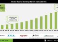
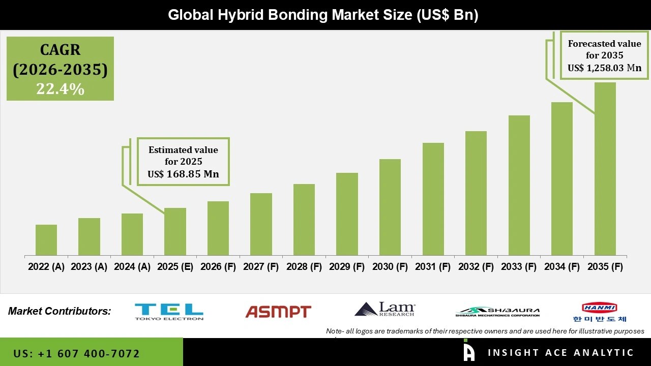
The Global Hybrid Bonding Market is valued at US$ 168.85 Mn in 2025 and it is expected to reach US$ 1,258.03 Mn by 2035, with a CAGR of 22.4% during the forecast period of 2026-2035.
Get Free Access to Demo Report, Excel Pivot and ToC: https://www.insightaceanalytic.com/request-sample/3483
Hybrid bonding technology is an advanced semiconductor manufacturing process that combines metal-to-metal and dielectric bonding techniques for wafer integration and chip stacking. Compared with traditional interconnection methods such as wire bonding and flip-chip packaging, hybrid bonding enables higher interconnect density, improved electrical performance, and greater thermal efficiency. As a result, it has become increasingly important in advanced 3D packaging applications used in high-performance electronic devices.
The hybrid bonding market is experiencing strong growth as the technology becomes a critical enabler of next-generation semiconductor packaging. This sophisticated interconnect approach, which forms direct copper-to-copper connections between stacked dies, is increasingly necessary to meet the density, speed, and efficiency requirements of modern computing systems. Market expansion is being driven by the growing adoption of high-bandwidth memory (HBM), 3D integrated circuits, and chiplet-based architectures in data centers and AI accelerators, where conventional solder-based packaging methods are no longer sufficient to deliver the required performance and power efficiency.
Leading semiconductor manufacturers are actively incorporating hybrid bonding capabilities into their production strategies, moving the technology beyond niche applications such as CMOS image sensors into mainstream high-performance computing environments. As the industry advances toward greater heterogeneous integration and more efficient memory architectures, hybrid bonding is expected to become a core component of advanced semiconductor manufacturing. Its long-term growth outlook remains closely linked to the continued expansion of AI hardware and increasing demand for faster, more energy-efficient electronic systems.
Read Comprehensive Report Overview: https://www.insightaceanalytic.com/report/hybrid-bonding-market/3483
List of Prominent Players in the Hybrid Bonding Market:
- Applied Materials, Inc.
- EV Group (EVG)
- Tokyo Electron (TEL)
- ASMPT
- SUSS MicroTec SE
- Besi
- Kulicke & Soffa Industries, Inc.
- TORAY ENGINEERING Co., Ltd.
- KLA Corporation
- Lam Research Corporation
- SHIBAURA MECHATRONICS CORPORATION
- DISCO Corporation
- BEIJING U-PRECISION TECH CO., LTD
- Hanmi Semiconductor
- Onto Innovation
Market Dynamics
Drivers
The hybrid bonding market is being driven by the increasing need for advanced thermal management solutions in high-power applications, the growing adoption of next-generation semiconductor packaging technologies, and rising demand for smaller, more energy-efficient devices across the consumer electronics and automotive sectors. Hybrid bonding has rapidly emerged as a critical enabling technology for advanced semiconductor integration, with expanding use in 3D packaging and heterogeneous integration applications.
This process enables superior alignment precision, reduced interconnect pitch, and improved electrical performance. In high-volume manufacturing environments, interconnect pitches as low as 10 micrometers are now being achieved. In addition, increasing global demand for smartphones, AI accelerators, and high-performance computing systems is significantly supporting market expansion. Manufacturers are increasingly implementing wafer-to-wafer and die-to-wafer bonding methods to achieve finer interconnections while enabling smaller chip sizes and enhanced performance.
Challenges
Despite strong growth potential, the market faces several operational and technical challenges. Hybrid bonding processes are highly sensitive to yield performance at advanced technology nodes and require ultra-clean surfaces, precise alignment, and complex process controls. Scaling production while maintaining sub-micron alignment accuracy remains a major challenge for industry participants.
Even minor inconsistencies in wafer flatness or particle contamination can lead to bonding defects and material losses, particularly in large-scale manufacturing. Maintaining consistent quality across multiple production lines requires continuous calibration, advanced metrology systems, and stringent cleanroom standards, all of which increase operating costs and complexity.
Adoption may also be slower among smaller foundries and outsourced semiconductor assembly and test (OSAT) providers due to limited access to skilled personnel, challenges associated with high-volume production scaling, and integration issues with existing fabrication lines. Furthermore, compatibility concerns and the absence of standardized interfaces, materials, and process flows across the semiconductor ecosystem continue to represent key barriers to broader market adoption.
Regional Trends
Asia Pacific is expected to register the fastest growth in the hybrid bonding market, supported by the region’s strong leadership in semiconductor manufacturing. Major chip producers in Taiwan, South Korea, and China are increasingly adopting 3D integrated circuits, high-bandwidth memory, and chiplet-based architectures for AI and high-performance computing applications.
Taiwan remains a key market due to its advanced foundry capabilities and continued investments in next-generation packaging technologies. As demand for smaller, more powerful, and energy-efficient electronic components continues to rise, hybrid bonding is becoming an essential technology for future semiconductor integration across the Asia Pacific region.
Add our site to Google Preferred Sources for quality content: https://google.com/preferences/source?q=insightaceanalytic.com
Segmentation of Hybrid Bonding Market-
By Equipment Type-
- Wafer Bonders
- Surface Prep Tools
- Inspection & Metrology Tools
- Cleaning & CMP Systems
By Bonding Type –
- Copper-to-Copper (Cu-Cu)
- Copper-to-Pad/Metal-to-Pad
- Others
By Integration Level-
- 5D Packaging
- 3D Stacked ICs
- Heterogeneous Integration
By Process Flow-
- Front-end
- Back-end
By Application-
- Memory & Storage
- Computing & Logic
- Connectivity & Communications
- Sensing & Interface
- Others
By Packaging Architecture-
- Wafer-to-Wafer (W2W)
- Die-to-Die (D2D)
- Die-to-Wafer (D2W)
By End-user-
- Consumer Electronics
- IT & Telecommunications
- Automotive
- Industrial Automation
- Healthcare & Medical
- Aerospace & Defense
- Others
By Region-
North America-
- The US
- Canada
Europe-
- Germany
- The UK
- France
- Italy
- Spain
- Rest of Europe
Asia-Pacific-
- China
- Japan
- India
- South Korea
- South East Asia
- Rest of Asia Pacific
Latin America-
- Brazil
- Argentina
- Mexico
- Rest of Latin America
Middle East & Africa-
- GCC Countries
- South Africa
- Rest of Middle East and Africa
Customize this Study according to your Requirements @ https://www.insightaceanalytic.com/customization/3483
About Us:
InsightAce Analytic is a market research and consulting firm that enables clients to make strategic decisions. Our qualitative and quantitative market intelligence solutions inform the need for market and competitive intelligence to expand businesses. We help clients gain competitive advantage by identifying untapped markets, exploring new and competing technologies, segmenting potential markets and repositioning products. Our expertise is in providing syndicated and custom market intelligence reports with an in-depth analysis with key market insights in a timely and cost-effective manner.
Contact us:
InsightAce Analytic Pvt. Ltd.
Visit: https://www.insightaceanalytic.com/
Tel : +1 607 400-7072
Asia: +91 79 72967118
info@insightaceanalytic.com